
The rapid evolution of artificial intelligence and high-performance computing has placed unprecedented demands on semiconductor architecture, leading to a critical bottleneck often referred to as the "memory wall." While the industry has responded with the development of High-Bandwidth Memory (HBM), the mere provision of massive data throughput is increasingly proving insufficient to meet the real-time processing requirements of modern System-on-Chip (SoC) designs. To understand this challenge, one might visualize a metropolitan highway during peak rush hour. While increasing the number of lanes—analogous to increasing bandwidth—allows for a higher volume of vehicles to move simultaneously, it does not inherently guarantee a faster commute. If the exits are poorly distributed, if the distance to be traveled remains excessive, or if traffic continues to flood the system beyond its management capacity, congestion persists. In the realm of silicon, even the most robust HBM systems can suffer from inefficiencies if the data movement is not managed through a sophisticated memory hierarchy.
The Architectural Challenge: Bandwidth vs. Latency
In the current semiconductor landscape, the distinction between bandwidth and latency has become a primary focus for architects. Bandwidth defines the total volume of data that can be moved over a specific period, whereas latency measures the time required for a single request to be fulfilled. High-Bandwidth Memory, specifically the latest HBM3E standards, offers a massive "pipe" for data, yet every request that must leave the compute die to fetch data from an external memory stack incurs a significant time penalty.
When a compute engine—be it a CPU, GPU, or Neural Processing Unit (NPU)—is forced to wait for data to return from external memory, it enters "idle cycles." These cycles represent wasted computational potential. In complex AI workloads, where data access patterns are often unpredictable or involve frequent reuse of the same data sets, these round trips to external HBM can become the primary performance bottleneck. This phenomenon occurs because HBM systems can effectively hide bandwidth inefficiencies behind their massive throughput, yet they remain vulnerable to the delays inherent in off-chip communication. Without a mechanism to keep reusable data closer to the processing cores, the system suffers from poor data locality and repeated, avoidable trips across the silicon interface.
The Evolution of Memory Hierarchy: A Chronology of Performance
The quest to balance capacity, speed, and cost has led to a tiered memory hierarchy that has evolved significantly over the last two decades. To contextualize the current role of Last-Level Cache (LLC), it is necessary to look at the progression of memory technologies:
- The DDR Era: Traditionally, system performance relied on Double Data Rate (DDR) SDRAM. While scalable in capacity, the physical distance between the CPU and the DIMM slots created significant latency and limited bandwidth.
- The Rise of GDDR: Graphics Double Data Rate (GDDR) memory, such as GDDR5 and the later GDDR6, was developed to provide the high throughput required for graphics processing. While it delivered significantly more bandwidth than traditional DRAM, the data still had to travel over relatively long PCB traces to reach the compute engines.
- The HBM Revolution: High-Bandwidth Memory (HBM) moved the memory stacks into the same package as the SoC, connected via a silicon interposer. This dramatically increased available bandwidth and reduced the physical distance data had to travel, yet the data still resided on a separate die from the logic.
- The Integration of LLC: As AI models grew in complexity, architects realized that even "in-package" memory was too far for certain high-frequency tasks. This led to the integration of large, on-chip Last-Level Caches (LLC) using SRAM (Static Random-Access Memory).
Today, the most advanced SoCs utilize a combination of these tiers. HBM3E provides the bulk storage and throughput for massive AI models, while on-chip SRAM, configured as an LLC, acts as a high-speed buffer that captures frequently accessed data before it ever has to leave the compute die.
Quantitative Analysis: The Impact of LLC on System Latency
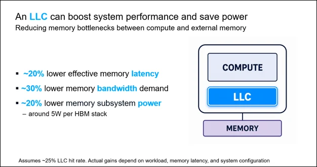
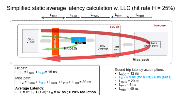
Recent performance analysis conducted by industry experts, including researchers at Arteris, provides concrete data on the benefits of integrating a configurable LLC into the memory subsystem. In a standard high-performance SoC environment, the average memory latency for a request traveling to external memory is approximately 83 nanoseconds (ns). This delay accounts for the time taken to traverse the Network-on-Chip (NoC), exit the die through the memory controller, access the HBM stack, and return.
By implementing a Last-Level Cache, such as the Arteris CodaCache IP, a significant portion of these requests can be satisfied on-chip. The data indicates that even with a modest cache hit rate of 25%—meaning only one in four data requests is found in the LLC—the average system latency drops from 83 ns to 67 ns. This represents a performance improvement of more than 20% in terms of responsiveness.
This reduction in latency directly translates to higher utilization of the compute engines. When the NPU or GPU spends 20% less time waiting for data, it can complete more operations per second, effectively increasing the "usable" performance of the silicon without requiring a change in the underlying HBM technology or clock speeds.
Technical Specifications: GDDR5 vs. HBM3E vs. On-Chip SRAM
To assist designers in making informed trade-offs, it is essential to compare the primary roles and engineering takeaways of current memory tiers:

- GDDR5 (External Subsystem): Primarily used for graphics and basic accelerators. While it offers better bandwidth than standard DRAM, the long physical paths to the compute engine remain a drawback for latency-sensitive AI applications.
- HBM3E (In-Package): This is the current gold standard for AI and High-Performance Computing (HPC). It provides extremely high throughput. However, the engineering takeaway is that data must still leave the compute die, which consumes power and adds latency.
- On-Chip SRAM (LLC): Positioned directly on the compute die, close to the processors. It serves as the fastest access path in the hierarchy. Its primary role is to reduce the number of trips to external memory, converting theoretical bandwidth into actual system throughput.
Strategic Implementation: CodaCache and the Modern NoC
The implementation of an LLC is not a one-size-fits-all solution; it requires a highly configurable IP that can be tailored to the specific needs of the SoC. Solutions like CodaCache by Arteris are designed to sit in the LLC path between upstream interconnect traffic and downstream memory access. This positioning allows the cache to monitor all data requests moving through the system.
In complex SoCs characterized by irregular access patterns or high contention among multiple compute engines, the LLC serves as a "traffic regulator." By keeping high-value, reusable data local, the LLC reduces the pressure on the external memory subsystem. This is particularly vital in multi-core environments where different engines (e.g., a GPU and an NPU) might be competing for the same HBM channels. The LLC can satisfy requests for shared data sets locally, preventing the memory controller from becoming a bottleneck.
Furthermore, the integration of LLC IP is often paired with advanced Network-on-Chip (NoC) solutions, such as FlexGen or Ncore cache-coherent interconnects. This synergy ensures that data remains consistent across all processing elements while minimizing the power-hungry activity of the external memory interface.
Power Efficiency: The Hidden Advantage of Data Locality
While latency and bandwidth are the most frequently cited metrics, power consumption is an equally critical factor in modern semiconductor design, especially in data centers where thermal management is a primary cost driver. Every transaction that leaves the compute die to access HBM requires significant energy. Moving data across a silicon interposer to an external stack is orders of magnitude more expensive in terms of picojoules per bit (pJ/bit) than accessing an on-chip SRAM.
By increasing the cache hit rate through an efficient LLC, designers can significantly reduce the total power profile of the SoC. A high hit rate means fewer HBM cycles are activated, reducing the energy spent on the memory interface and the HBM stacks themselves. In AI applications where billions of parameters are processed, the cumulative energy savings of reducing off-chip traffic can be the difference between a chip that meets its thermal design power (TDP) and one that requires expensive, specialized cooling solutions.

Industry Implications and Future Outlook
The industry’s move toward "chiplet" architectures further underscores the importance of a robust memory hierarchy. As compute engines and memory are increasingly split into separate chiplets, the "inter-chip" latency will only become more challenging. In this context, the Last-Level Cache will serve as the essential glue that maintains performance across fragmented silicon.
Market analysts suggest that the next generation of AI accelerators will not compete solely on the amount of HBM they can stack around a processor, but on the intelligence of their on-chip memory management. The systems that achieve the highest "performance per watt" will be those that use their bandwidth wisely—minimizing avoidable trips to external memory and ensuring that compute engines are never left idling.
In summary, the HBM era has provided the industry with the "highway lanes" necessary for the AI revolution. However, the integration of Last-Level Cache IP, such as Arteris CodaCache, provides the "efficient traffic management" required to make those lanes useful. By reducing average latency by over 20% and significantly lowering power consumption, the LLC has transitioned from a luxury to a fundamental necessity in high-performance SoC design. The future of computing belongs to architectures that prioritize not just the volume of data movement, but the efficiency and locality of every bit processed.
