
The global semiconductor industry is currently undergoing a seismic shift in architectural philosophy, transitioning from traditional monolithic System-on-Chip (SoC) designs toward heterogeneous integration through chiplet technology. As the physical limits of Moore’s Law become increasingly difficult and expensive to overcome, the assembly of pre-designed or third-party Intellectual Property (IP) onto high-performance interposers and advanced 2.5D and 3D integrated circuits (3D-ICs) has emerged as the primary path forward for high-performance computing. This transformation is not merely a change in physical layout but a fundamental reimagining of the design-to-manufacturing workflow. Industry leaders, including Siemens Digital Industries Software, are now advocating for a robust, system-centric methodology to address the limitations of legacy tools which were primarily built for single-die devices. By adopting System-Level Technology Co-Optimization (STCO), engineers can now manage the staggering complexity of devices that feature tens of millions of pins and sophisticated vertical stacking.
The Historical Context and the Move Toward More-than-Moore
For decades, semiconductor advancement relied on "geometric scaling"—shrinking transistors to pack more onto a single piece of silicon. However, as nodes reached the 5nm, 3nm, and now 2nm thresholds, the cost of designing monolithic dies skyrocketed, while yield rates for large chips began to plummet. This economic and physical wall necessitated the "More-than-Moore" era, where performance gains are achieved through advanced packaging rather than just transistor shrinkage.
Heterogeneous integration allows for the mixing and matching of different process nodes within a single package. For instance, a 3nm processor can be paired with 7nm I/O controllers and high-bandwidth memory (HBM), all sitting on a common interposer. While this offers advantages in power efficiency and cost, it introduces a "connectivity explosion." Traditional design tools, which relied on manual spreadsheet-based tracking for pin assignments, are now obsolete in an era where a single device may house over 50 million total pins.
The Foundation of the 3D Digital Twin
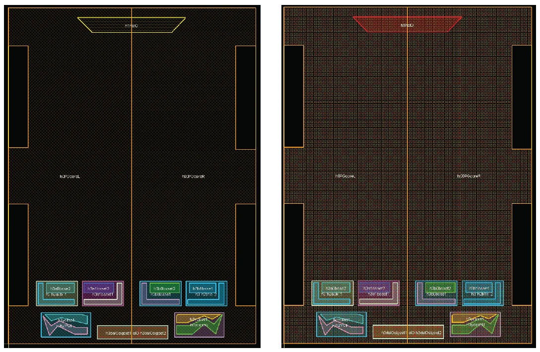
The cornerstone of modern 3D-IC design is the creation of a comprehensive 3D digital twin. This digital model acts as a single, authoritative source of truth for the entire system, encompassing the silicon dies, chiplets, bridges, interposers, substrates, and the Printed Circuit Board (PCB). The integration process begins with the aggregation of diverse design IP. This is a significant challenge because data often arrives in varied formats and from different vendors.
To combat the risks associated with manual data entry, the industry is moving toward standardized formats such as IEEE 3Dblox, OCP CDX, and JEDEC JEP30 Part Models. These standards are designed to facilitate seamless data exchange across the semiconductor ecosystem. By utilizing a tool like the Siemens Innovator3D IC Integrator, designers can construct a system-level netlist that serves as the blueprint for subsequent physical verification and multiphysics analysis. This digital twin allows for "pathfinding," where engineers can explore different integration scenarios to find the optimal balance of Power, Performance, Area, Cost, and Reliability (PPAC&R).

Chronology of the 3D-IC Design Workflow
The transition from concept to a finalized 3D-IC follows a specific chronological path designed to minimize iterative cycles and ensure "first-time-right" manufacturing.
- IP Aggregation and Revision Control: Designers collect netlists, spreadsheets, and Verilog files. Given the concurrent nature of modern design, where multiple teams work on different chiplets simultaneously, robust version control is essential to ensure that the latest IP is always being utilized without overwriting critical data.
- Interface and Bump Array Construction: Using hierarchical design principles, complex structures are broken down into manageable building blocks. Instead of flat models, designers use parameterized pin regions. For example, an interposer connecting four HBM modules can be constructed using repeatable die-to-die building blocks, allowing updates to be processed in seconds rather than days.
- Language-Based Netlist Creation: As designs exceed millions of connections, the industry is shifting from spreadsheets to language-based design (such as Verilog RTL). This allows for the use of bus notation, which is significantly more efficient for high-width interfaces like those found in AI accelerators.
- Bridge and Interposer Instantiation: Once the connectivity is verified, silicon bridges and interposers are derived as a function of the devices they connect. This ensures that the wiring layers—the "highways" of the chip—are perfectly aligned with the chips they serve.
Technical Challenges: Power, Thermal, and Connectivity
The shift to 3D-ICs introduces three primary physical hurdles: power delivery, heat dissipation, and routing congestion.
Power Delivery Networks (PDN): As multiple dies are stacked or placed in close proximity, the demand for stable voltage increases. Modern 3D-ICs often require dedicated metal layers for power distribution to prevent voltage drops (IR drop) that can lead to logic errors. Predictive analysis is now used early in the design phase to identify "copper scarcity" and ensure that the current draw of high-performance chiplets does not exceed the capacity of the package’s substrate.

Thermal Management: Vertical stacking is a double-edged sword. While it reduces the distance signals must travel, it traps heat between layers. Thinning the silicon dies to allow for shorter vertical interconnects (Through-Silicon Vias or TSVs) actually increases lateral thermal resistance. Tools such as Calibre 3DThermal are now integrated into the pathfinding process, allowing engineers to visualize heat gradients before the design is finalized. Failure to address thermal issues early can lead to "thermal throttling," where the chip must slow down to avoid melting, effectively nullifying the performance gains of the 3D architecture.
Route Resource Planning: In a package with 50 million pins, traditional "rip-up and retry" routing is impossible. Designers now use hierarchical connectivity bundles, or "data paths," to plan routes at a high level. This ensures that critical signal groups—such as those for UCIe or HBM interfaces—have dedicated "lanes" on the substrate, preventing congestion and maintaining signal integrity.
Data-Driven Insights: The Density Revolution
Supporting data highlights the scale of this technological leap. In current high-end AI and hyperscaler applications, hybrid and direct bonding technologies are enabling bump densities of 25,000 to 50,000 per square millimeter. This density is necessary to support the massive bandwidth requirements of Large Language Models (LLMs) and complex simulations.

According to industry analysts, the move to 3D-IC can reduce the footprint of a system by up to 40% while improving power efficiency by 25-30% compared to traditional PCB-based integration. However, these gains are only achievable if the design teams can maintain "digital continuity"—a seamless flow of data from the initial floorplan to the final sign-off.
Official Responses and Industry Standardization
The push for standardized 3D-IC workflows has seen significant buy-in from major Electronic Design Automation (EDA) providers and foundries. Siemens, for instance, has positioned its Innovator3D IC product family as a "cockpit-driven environment" that allows for STCO across silicon, package, and PCB domains.
Industry groups like the Open Compute Project (OCP) have emphasized that without standardized chiplet interfaces (like UCIe), the vision of a "plug-and-play" chiplet marketplace cannot be realized. Official statements from major foundries indicate that 3D-IC packaging capacity is being expanded at a record pace to meet the demands of AI chip designers, further underscoring the necessity of these advanced design methodologies.

Broader Impact and Future Implications
The implications of streamlined 3D-IC design extend far beyond the semiconductor industry. By lowering the barrier to entry for complex system-in-package (SiP) designs, more companies will be able to develop custom silicon tailored to specific applications, such as autonomous driving, edge computing, and personalized medicine.
The "shift-left" approach—moving analysis and verification earlier in the design cycle—not only reduces time-to-market but also significantly lowers the cost of failure. In an environment where a single 3nm tape-out can cost hundreds of millions of dollars, the ability to predict thermal and electrical behavior via a 3D digital twin is a financial imperative.
As the industry looks toward the next decade, the integration of Machine Learning (ML) and Artificial Intelligence (AI) into the EDA tools themselves will likely be the next step. Algorithms are already being used to optimize pin assignments and floorplans, tasks that are becoming too complex for human engineers to manage alone. The future of semiconductor integration lies in this synergy between human architectural intent and automated, system-level optimization, ensuring that the next generation of computing devices continues to meet the world’s insatiable demand for performance.
